Programmable VLA Inference Accelerator — from workload evidence to chip architecture
Track 5F · AI Chip Design · Professional design studio
Design a programmable, memory-efficient accelerator around useful robot behavior.
Design objective: complete the required robot tasks with less compute-system energy, predictable observation-to-action timing, and a declared task-quality budget. The target is local VLA inference with programmable tensor/vector execution, explicit memory management, and a compiler/runtime designed alongside the hardware.
This course develops the supplied accelerator proposal into a research-backed engineering sequence. It preserves the proposal's central goal and adds the missing steps needed to test it: model trace contracts, capacity versus traffic, cold/warm residency, tile shape effects, valid caching, shared-resource scheduling, statistical evaluation, and implementation evidence.
Research cutoff: October 14, 2026. Specifications and published results are attributed to primary sources in hardware evidence and model/research evidence. They are distinct from the original analytical exercises and CPU results in this course. Later October developments are outside this snapshot.
Contribution to the roadmap: VLA foundations defines the policy; inference optimization establishes the baseline; this course turns those measurements into the accelerator, compiler, and runtime requirements for the physical-AI SoC.
What the research changes in the proposal
- Use a diverse executable workload set. Flow-based, autoregressive-action, and cascade policies stress different matrix shapes, state, and repeated work. Public announcements and partner-only models are comparison context until an executable artifact is available.
- Preserve benchmark conditions. GR00T's published rates describe new action chunks under stated camera/denoising settings. They are vendor results with incomplete system metadata; its two official pages also differ slightly on Orin eager performance. See Lecture 01.
- Model memory before choosing peak arithmetic. A 300M-parameter, packed-4-bit expert requires 150 MB before metadata. Partial residency has a calculable benefit; it does not imply the whole expert fits in tens of MiB of SRAM.
- Separate format, execution, and behavior. A low-bit checkpoint, a native arithmetic kernel, and preserved closed-loop quality need separate evidence. Research on one policy/precision pair does not establish support for another.
- Make scheduling and programmability concrete. Specify legal tile boundaries, memory arbitration, vector operations, state lifetime, command ABI, fallback, and action expiry.
The initial 20–40 W, 16–32 GB external memory, 16–64 MiB SRAM, and 10–30 fresh evaluations/s envelope is a design-space hypothesis. The course does not assert that all its bounds are simultaneously feasible, nor choose a process node before an implementation study.
Prerequisites and access routes
You should be able to trace tensor shapes through one policy, explain a roofline bound, distinguish a model output from a controller command, and read basic Python/C++. Use the VLA CPU labs, framework courses, and compiler stack to fill gaps. RTL/FPGA experience is needed for the hardware extension, not for the initial architecture analysis.
| Access | What you can complete | Correct claim |
|---|---|---|
| CPU laptop, Python 3.10+ | All bundled labs, trace arithmetic, format/ABI design, candidate analysis | Reproduced analytical fixture and design study |
| Compatible GPU and usable model | Reference tracing, kernel/quality/memory measurements | Results for the named model, runtime, and device |
| Supported Isaac setup | Paired task trials, freshness/failure injection | Closed-loop simulation evidence |
| FPGA/RTL tools | Selected datapath, interface, driver, and recovery tests | Implemented prototype evidence |
| Physical-design/IP access | Named-process feasibility and implementation study | PPA estimates at documented corners, followed by separate silicon evidence |
Start with the lab guide. The bundled labs require no GPU, simulator, network, checkpoint download, or third-party Python package.
Lecture sequence and artifact handoffs
| # | Lecture | Pass to the next lesson |
|---|---|---|
| 01 | Design brief and competing baselines | Task, quality, power, latency, and comparison contract |
| 02 | Workload atlas and trace contract | Versioned shapes, dependencies, repeated work, and lifetimes |
| 03 | Programmable tensor and vector tiles | Tile/operation candidates and shape-efficiency analysis |
| 04 | Memory residency and traffic | Capacity/traffic ledger with cold/warm and SRAM assumptions |
| 05 | Precision and valid reuse | Numerical-format and cache-invalidation contracts |
| 06 | Compiler, runtime ABI, and SoC integration | Lowered command path, ownership, fallback, and completion rules |
| 07 | Scheduling for fresh actions | Blocking, overload, and observation-age evidence |
| 08 | Energy, task quality, and honest comparisons | Paired evaluation, raw energy, timing, and uncertainty |
| 09 | Prototype to silicon feasibility | Executable vertical slice and implementation evidence matrix |
| 10 | Capstone design defense | Reviewed accelerator proposal and next SoC integration gate |
First worked result
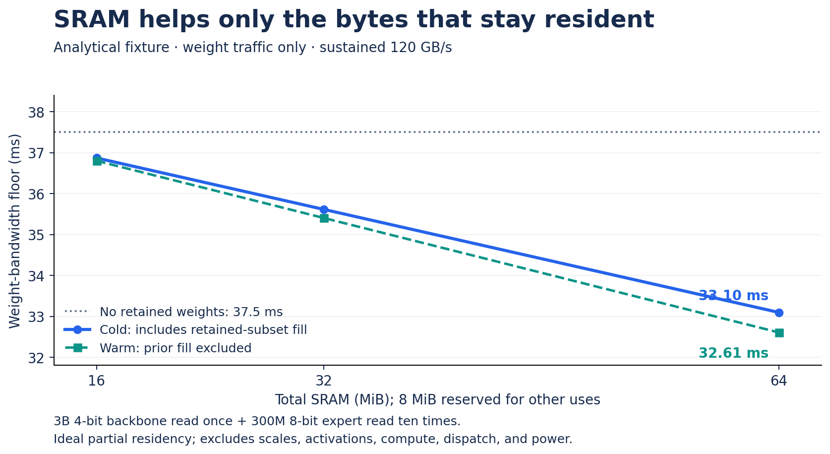
For a synthetic policy, a 3B packed-4-bit backbone read once costs 1.5 GB. A 300M 8-bit expert read ten times costs 3 GB. Total weight traffic is 4.5 GB per evaluation; at a stated sustained 120 GB/s, weight movement alone requires 37.5 ms under the no-residency assumptions. At 20 evaluations/s, that is 90 GB/s of weight traffic.
The expert is repeated; the backbone is not. The 1.8 GB weight capacity and 4.5 GB per-evaluation traffic answer different questions. Scales, activation/state traffic, compute, queueing, and dispatch are absent from this first calculation and enter later exercises.
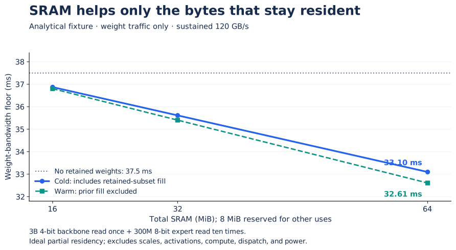
Use the CPU lab to reproduce the curve, then identify the omitted cost most likely to matter for your policy. PNG.
How to study and complete the course
For each lecture, predict the worked result, reproduce it, change one assumption, and submit the named handoff. Use the answered self-checks after attempting them without notes. Keep all handoffs in one project repository so a compiler or SRAM choice can be traced back to an actual workload.
Completion requires a reviewed requirement sheet, a workload/traffic dossier, a supported operation/precision set, a compiler/runtime ABI, a scheduling/freshness analysis, a declared evaluation protocol, and one executable result at your available implementation level. The capstone rubric distinguishes a course pass from an unproven product claim.
Next: Physical AI Design Studio → full SoC capstone. Extend the accelerator prototype with Linux, sensors, wireless, and controller integration while retaining the same task and evidence contracts.
Connect the model to the hardware worksheet
The model-to-hardware CPU lab reuses a trained scalar action model from the robotics course. Export and reload its computation graph, capture actual CPU calls, then derive parameter storage, repeated work, and proposed tile-padding costs. Keep its synthetic task and CPU execution scope in your design report.