In the first post I built a TIP5 hashing accelerator for Neptune Cash on AWS EC2 F2 — eight AMD Virtex UltraScale+ FPGAs you rent by the hour. The next step wasn’t to leave UltraScale+ behind; it was to bring it onto hardware I owned. The board is an Osprey E300: three VU35P UltraScale+ FPGAs do the hashing, and a small Zynq 7010 does nothing but control them — program their bitstreams and relay UART.
That split is the whole story of this post. The VU35P is a Virtex part: it has no processor at all. So the miner’s controller — the thing that receives a job, sequences the hash cores, and reports a winning nonce — can’t live on a CPU. It has to be logic, in the programmable fabric. No ARM, no soft CPU, no Linux in the data path: a soft UART, a control state machine, and the hash cores, all in PL, driven over a serial wire. The code is in ai-hpc/tip5-neptune under Osprey/.
Table of contents
Open Table of contents
Two kinds of FPGA, two jobs
The Osprey E300 is a multi-FPGA board with a clean division of labor:
┌──────────────┐  SSH/XVC/UART  ┌──────────────────┐  JTAG program  ┌────────────────────────┐
│  Dev PC      │◄──────────────►│   Zynq 7010      │◄──────────────►│  3× VU35P UltraScale+  │
│  + host app  │                │   controller     │  UART runtime  │  fpga1 · fpga2 · fpga3 │
│  (SSH/UART)  │                │   Linux + XVC    │                │  TIP5 miner in pure PL │
└──────────────┘ └──────────────────┘ └────────────────────────┘- The compute: three VU35P UltraScale+ (
xcvu35p-fsvh2104-2LV-e). Each one runs a self-contained TIP5 miner bitstream — soft UART, control FSM, and a bank of hash cores. This is where every hash happens. - The controller: one Zynq 7010. It runs Linux, programs all three VU35Ps over a JTAG chain (an XVC server plus a
loadalltool), and relays UART to each at runtime — the three FPGAs appear to it as/dev/uio8,/dev/uio9,/dev/uio10. It does zero hashing. It is a conduit, nothing more.
It’s worth being clear about this, because it’s the part I got wrong in my own head at first: the Zynq is not the miner. It’s the cheap brain that loads bitstreams onto the real silicon and shuttles bytes. The interesting engineering — and everything below — is on the VU35P side.
Why the controller lives in PL, not on a processor
On a Zynq you’d reach for the ARM Processing System (PS): boot Linux, run control software, let the PS be the AXI master that pokes registers on your PL IP. The VU35P doesn’t give you that option — it’s a Virtex UltraScale+ with no PS. And I deliberately didn’t paper over the gap with a MicroBlaze soft CPU either. The controller is a hand-built state machine in logic.
Four reasons that turned out to matter, in order:
- Portability. A PL-only design isn’t tied to any one part. The same RTL — soft UART, control FSM, TIP5 cores — runs on the VU35P here and on the VU47P from the F2 build, because none of it assumes a processor. One codebase, three classes of silicon.
- No boot stack. No first-stage bootloader, no U-Boot, no PetaLinux, no DDR bring-up on the compute FPGA. Configure the PL and it runs. An order of magnitude fewer things to get wrong.
- Determinism. No OS jitter, no interrupt latency, no scheduler. The control FSM advances on a clock edge, every clock edge.
- A clean truth test. If the hash cores produce correct digests when driven by a dumb FSM over a UART, the cores are correct — there’s no software layer to hide a bug in.
The catch is that you have to build the thing a CPU would have done. Something has to be the AXI master. Something has to receive bytes, parse commands, and sequence the cores. On a normal Zynq that’s the ARM; on the VU35P it’s logic — and that’s the interesting part of the design.
The design: a soft UART, an AXI master, and a control FSM
I brought the VU35P bitstream up in three layers, and the commit history still shows the order.
Layer 1 — get a byte in and a byte out. uart_rx_tx.v is a from-scratch soft UART: oversampled RX to find the middle of each bit, start/stop framing, a configurable baud divisor off the fabric clock. The first milestone was an echo — type a character into a serial terminal, watch the fabric send it back. Unglamorous, but it proves the clocking, the pin constraints, and the framing all at once.
Layer 2 — make the UART the AXI master. This is the crux of “no processor.” axi_uart_tip5_master.v is an AXI master implemented in logic — a UART-driven state machine that issues AXI read/write transactions to the rest of the design, doing the job the PS does on an ordinary Zynq. I bootstrapped it with a series of axi_uart_hello_master variants (write a register, read it back, entirely over the serial link) before putting the hash cores behind it. There’s also a uartlite_bd.v path using AMD’s AXI UARTLite IP — which the Zynq reaches over UIO — but the fully custom master is the one with no hidden dependency on a processor to configure it.
Layer 3 — the controller and the cores. tip5_uart_axi_controller.sv is the command FSM: it receives a UART packet, decodes a small command set — load a job digest, set a nonce range, start, stop, read status, read the winning nonce — and sequences the hash units. The cores are the VU35P-optimized TIP5 pipeline in Osprey/vu35p_parallel_pipeline/ (tip5_vu35p_hash_optimized.sv), and tip5_kernel_mast_hash_pipelined.sv instantiates 7 parallel hash units per FPGA so the fabric is doing real work:
// Generate 7 hash units for parallel processing
genvar g;
generate
    for (g = 0; g < NUM_HASH_UNITS; g++) begin : gen_hash_units
        tip5_hash_unified u_hash (
            .clk(clk), .rst(rst),
            .nonce_in (nonce_base + g),   // each unit owns a slice of nonce space
            .digest_in(job_digest),
            .hit      (hit[g]),
            .result   (result[g])
        );
    end
endgenerate
The host side is correspondingly tiny and runs on the Zynq controller: host_uart.c opens each FPGA’s UART channel, sends a job and a nonce range, and polls for a hit. No kernel driver on the data path, no PCIe stack — just bytes on a wire landing directly in VU35P logic. With three FPGAs, the controller hands each one a disjoint slice of the nonce space and watches all three for a winner.
The hardest part: timing closure at 450 MHz
If one thing defined this project, it wasn’t the hash logic or the UART — it was timing closure. The TIP5 datapath is arithmetic-dense: a Goldilocks-field multiply is a 64×64→128-bit multiply followed by a reduction, the MDS layer is a 16×16 matrix of those, and the x⁷ power map chains several together. To make the miner worth running you want the fabric clock as high as it will go — I was pushing for 450 MHz and beyond — and at 450 MHz the clock period is ~2.2 ns, shorter than the propagation delay through even a modest slice of that arithmetic.
So every path has to be sliced into pipeline stages short enough to settle in a single cycle, and then placed and routed so the wires between stages don’t eat the budget on their own. (The fast clock comes from an MMCM multiplying up the board’s reference clock — the external 50 MHz input is the easy part; the 450 MHz internal clock is where the pain lives.) On the VU35P that routing problem is genuinely hard, because the part is a stacked-silicon (SSI) device: the fabric is split across two Super Logic Regions — SLR0 and SLR1 — and any path that crosses between them pays a real penalty through the limited SLL crossing routes. Here is the placed design — used logic in cyan, spread across both SLRs, with the HBM stacks along the bottom edge:
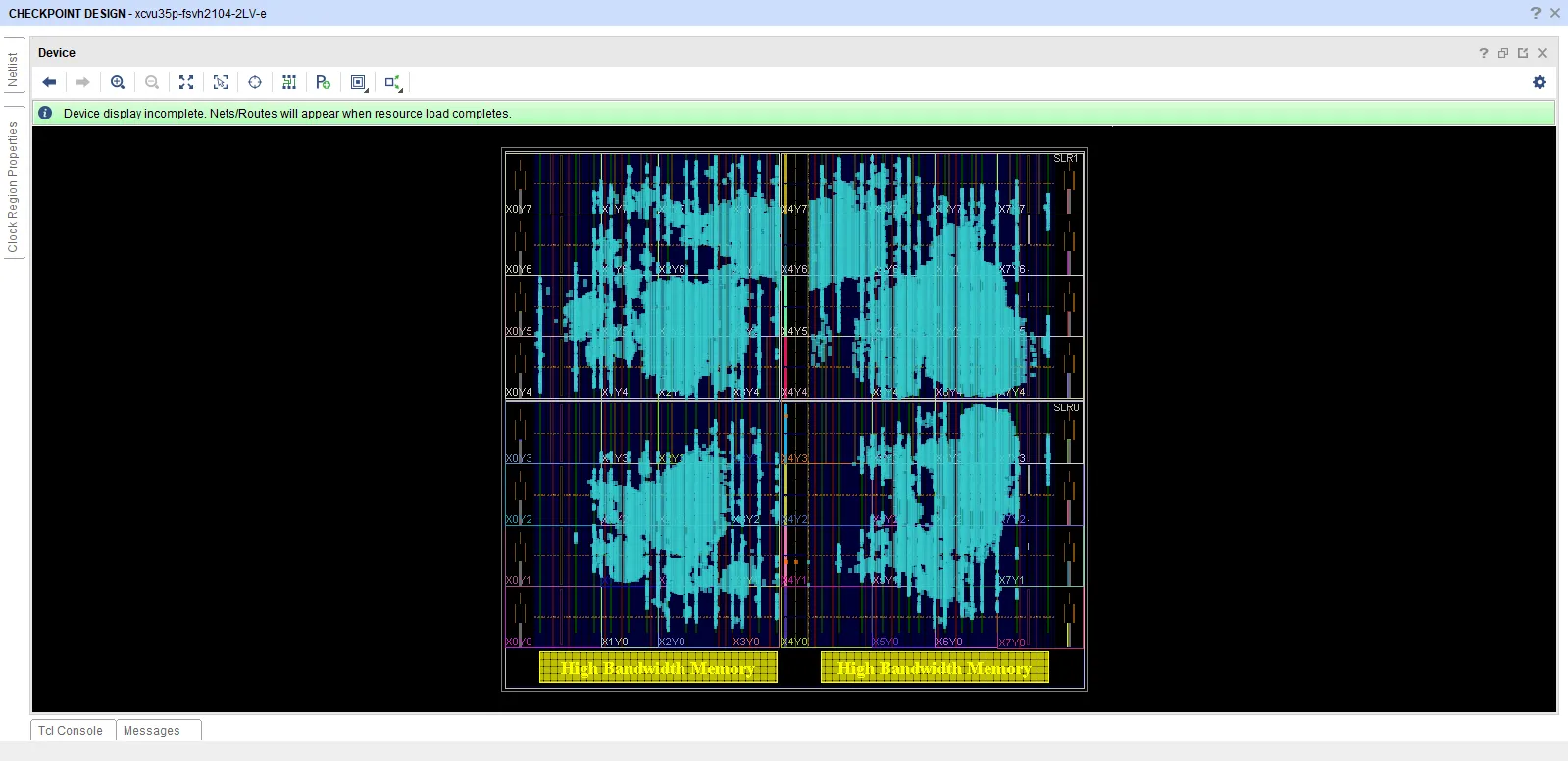
When a critical path lands across that SLR boundary at 450 MHz, you simply don’t make timing, and the report comes back with negative slack — a negative WNS (worst negative slack). A bitstream that fails timing isn’t one you can ship; it will hash incorrectly or not at all. So you go back, add a pipeline stage, floorplan the offending logic into a single SLR, or drop the clock — and run place-and-route again, an hour each time.
That loop is the real cost of FPGA development, and negative timing closure was the thing that hindered me most. It doesn’t just cost you the failed run; it caps how fast you can try things. Every architectural idea — a deeper MDS pipeline, a different multiplier mapping, more hash units per FPGA — has to survive timing before you know whether it helped, and finding out takes the better part of an hour. Six months of FPGA work was, more than anything, six months of waiting on timing reports.
The tactical tools help at the margin. Pinning related logic into one clock region with pblocks keeps a datapath from sprawling across the die (and across the SLR boundary); a dedicated clock route avoids a DRC that stops the build cold:
create_pblock pblock_uart
resize_pblock [get_pblocks pblock_uart] -add {CLOCKREGION_X1Y1:CLOCKREGION_X1Y1}
add_cells_to_pblock [get_pblocks pblock_uart] [get_cells -hierarchical {uartlite_bd_i}]
set_property CLOCK_DEDICATED_ROUTE BACKBONE [get_nets .../clk_in1_...]
(There’s a drc_error.txt and a literal “Fix DRC Error” commit in the repo — CLOCK_DEDICATED_ROUTE BACKBONE is the incantation you learn the hard way, when Vivado refuses to route a clock-wizard input that isn’t on a dedicated route.) An ILA (dbg_hub) in its own pblock gave me on-chip visibility when the UART framing was off by a bit. But these are damage control. The fundamental tax is that at 450 MHz on a two-SLR device, timing closure is the gate every change has to pass through — and it is slow.
Programming the VU35Ps through the Zynq controller
Here’s where the Zynq earns its keep. The three VU35Ps have no flash and no host bus of their own — they’re programmed over a JTAG chain that the Zynq drives. The Zynq runs Linux with an XVC (Xilinx Virtual Cable) server (jtag_xvcserver.c) bound to a UIO-mapped JTAG port, and a loadall tool pushes a bitstream over that chain onto the downstream FPGAs:
# copy each bitstream and the loader to the Zynq controller, then program over XVC/JTAG
scp e335_v1.bit loadall ubuntu@<board_ip>:~/
ssh ubuntu@<board_ip> './loadall /path/to/bitstreams/'
XVC also means a development PC running Vivado Hardware Manager can reach the VU35Ps over the network through the Zynq — open the target, program the device, even attach the ILA remotely, as if the FPGAs were on a local JTAG cable. For a single-FPGA bring-up I’d program one VU35P directly; for the real board, loadall flashes all three and the Zynq then relays UART to each. The Zynq is the only thing on the board with an OS, and its entire role is this: get bitstreams onto the UltraScale+ parts and move bytes to and from them.
What it taught me — and the wall I hit
Forcing the controller into PL was the best decision of the project for learning. I came out of it understanding soft UARTs, AXI mastering, clock-region floorplanning, DRC closure, and the JTAG/XVC programming path at a level I’d never have reached by leaning on a CPU and a Linux driver.
And it put the wall from the last section front and center: when timing closure gates every change and each attempt costs an hour of place-and-route, your iteration rate — not the silicon — is the bottleneck. By late summer the mining target was moving faster than I could close timing on it.
So I ran an experiment I expected to lose: reimplement the whole thing in CUDA on a single GPU and see how far I got in a month. That’s the third and final post — and it’s the reason there is no fourth FPGA post.